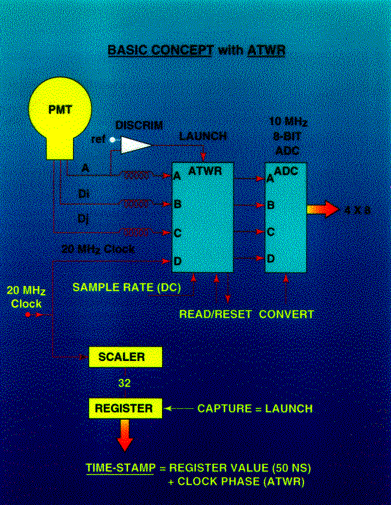
 The ATWR digitizes the anode and two dynodes signals for dynamic range.
The digitization generally takes place with a time step
of 0.3 to 1 nanosecond.
The ATWR digitizes the anode and two dynodes signals for dynamic range.
The digitization generally takes place with a time step
of 0.3 to 1 nanosecond.
An effort is currently under way to develop a "smart" optical module for
neutrino astronomy, incorporating a local CPU and a special chip called
the ATWR (analog transient waveform recorder).
The ATWR digitizes the anode and two dynodes signals for dynamic range.
The digitization generally takes place with a time step
of 0.3 to 1 nanosecond.
 (To the right is the digital optical module prototype with 2 km of coax.)
The ATWR is a custom integrated circuit developed at LBNL.
It is a monolithic multichannel device,
developed in 1.2 micron CMOS using switched-capacitor sample-and-hold
techniques.
(To the right is the digital optical module prototype with 2 km of coax.)
The ATWR is a custom integrated circuit developed at LBNL.
It is a monolithic multichannel device,
developed in 1.2 micron CMOS using switched-capacitor sample-and-hold
techniques.
 It is capable of sampling analog waveforms at easily programmable rates
from 0.3 to 3 GHz.
The sampling rate is determined by a single analog current input to the ATWR;
no external clocks are necessary.
Internally, an
edge-sensitive active delay line uses look-ahead and
4-way interleaving to develop the sample-and-hold clocks.
The sampling action is launched by applying a step to a control node.
It is capable of sampling analog waveforms at easily programmable rates
from 0.3 to 3 GHz.
The sampling rate is determined by a single analog current input to the ATWR;
no external clocks are necessary.
Internally, an
edge-sensitive active delay line uses look-ahead and
4-way interleaving to develop the sample-and-hold clocks.
The sampling action is launched by applying a step to a control node.
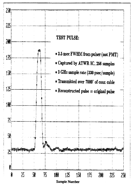
The analog sampling bandwidth is ~400 MHz, with ~10 bit signal/noise ratio. The analog information can be subsequently read out at MHz speeds, compatible with low-power high resolution ADCs, and allowing the waveform to be transmitted slowly over very long coax or twisted pair cables. (At left is a picture of a pulser test demonstrating the ATWR capabilities.) The ATWR power dissipation is less than 10 mW/channel (mostly the output buffer amps). The sampling action of the different input channels is phase-locked by the common internal structure of the delay line, so that all channels have identical sample apertures and speeds. An architecture based on the ATWR IC can take advantage of the low average duty cycle, avoid ultra-high speed clocks, and provide excellent performance with extremely low power dissipation.
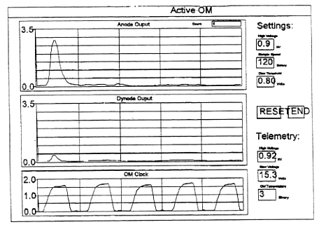 The ATWR has been incorporated into a prototype optical module by JPL engineers.
They pull off the signals from the anode of a photomultiplier tube, a dynode,
and a clock waveform, and input them into the three channels of the ATWR.
JPL has devised a way for the digital OM to operate with both upgoing data and
downgoing control signals using the same cable,
so that this module can be used as part of the AMANDA experiment
in a realistic field test.
(At right is shown the computer interface to the prototype OM,
with actual PMT waveforms displayed.)
We have constructed three additional modules with an improved communications
protocol,
and have installed two of them at the South Pole the 1996-1997 as part
of the AMANDA deployment.
The ATWR has been incorporated into a prototype optical module by JPL engineers.
They pull off the signals from the anode of a photomultiplier tube, a dynode,
and a clock waveform, and input them into the three channels of the ATWR.
JPL has devised a way for the digital OM to operate with both upgoing data and
downgoing control signals using the same cable,
so that this module can be used as part of the AMANDA experiment
in a realistic field test.
(At right is shown the computer interface to the prototype OM,
with actual PMT waveforms displayed.)
We have constructed three additional modules with an improved communications
protocol,
and have installed two of them at the South Pole the 1996-1997 as part
of the AMANDA deployment.
Some sample waveforms given by the DOM when sampled on the AMANDA trigger
are shown
in the accompanying figure.
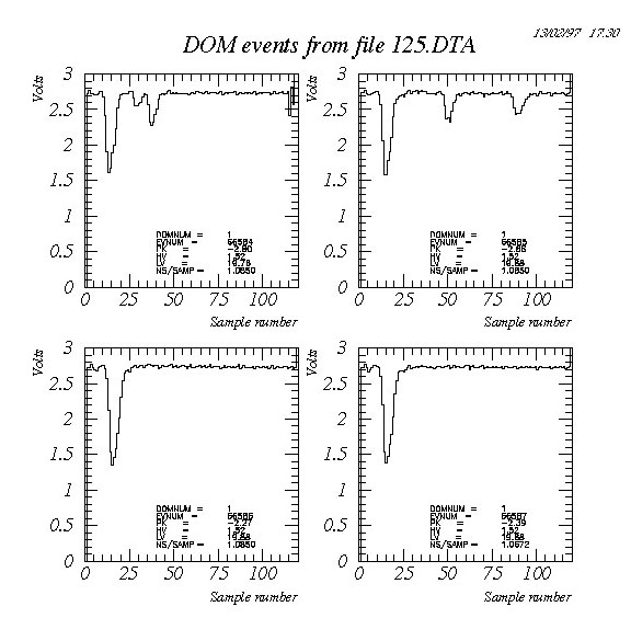 Note the interesting and complicated waveforms.
Reference:
"Technology Development for a Neutrino Astrophysical Observatory",
Lawrence Berkeley National Laboratory manuscript LBL-38321 UC-412, Feb. 1996.