Smoot Astrophysics Group
Data Acquisition System


Description:

      The data acquisition system (DAS) was designed to interface any experiment with up to 240 different analog or digital outputs to a computer. The DAS is a modular form built into single width NIM modules and a typical system is composed from five basic modules. One control module, one 16 input Analog Multiplexer / ADC, 16 input Analog Submultiplexers as required, Dual 16 bit Digital Word modules as required, and a serial to RS232 module if required.
      The address bus has 8 bits so after allocating 16 addresses for internal use, up to 240 distinct analog or digital inputs can be addressed.
      The bit or band rate ranges from 150 to 38.4k band. There is also a 32 bps position which meets a NASA serial data standard.
      The serial data output consists of a frame of 16 bit words sent seamlessly with a unique synchronization word to identify the start of each data frame.
      The control module has a slide switch to set the baud rate, also a EPROM in a zero insertion force socket. The data frame set-up is burnt into this EPROM and is arranged for analog or digital data in any order required. The DAS is powered through the control unit and requires plus or minus 15V. If the protective polarity reversal diodes are shorted out, the DAS will work on plus or minus 12V. The output connector has a serial data output line. There is also a opto-coupled BiPhase Serial data line powered from an internal isolated power supply.
      The Analog Multiplexer / ADC module has 16 differential inputs of FSD plus or minus 10V with a common mode rejection of 86 dB. The ADC limits hard at plus or minus 10V. There is no bleed over between channels with overloads of plus or minus 30V.
      The 16 input analog Submultiplexer module is used when there are more than 16 analog inputs. Each submultiplexer monopolizes one of the analog multiplexer / ADC module inputs.
      The Dual Digital Word module accepts 2 each 16 bit words (each 16 bit word could be made up of subdigital words for example two 8 bit words). Additional modules are added to meet the number of digital words.
      The serial to RS232 module takes the seamless serial data and synchronizes to the "sync word". Each 16 bit word is converted to RS232 format and can be sent to any computer with a special input port and the right software. Labview has been used successfully. A finite time is required for conversion so using this particular module the maximum DAS baud rate can only be 2.4k baud or less. The module outputs at 9.6k baud.
      The only connection between modules is via a 25 conductor flat cable with D type connectors crimped on as required. The modules do not have to sit side be side or in any particular order. Some may be separated from the others by up to 30' of cable. Greater separation might need cable ringing suppression devices at the end of the bus. The bus has many functions such as: 8 bit device address but, Power to modules ( + or - 15V, +5V), Bit Clock, Word Clock, "End of Data Frame" pulse, "Power-up Reset" pulse, "Common Serial Data Line" between modules, "Serial Data Output", "Odd/Even Frames", "Busy Line", and several ground wires paralleling sensitive data lines.
      An attempt was made to keep the power drain reasonably low for applications that must be powered from batteries. The measured current drains were as follows:


Module
Control
Analog Multiplexer/ADC
Analog Submultiplexer
Dual Digital Word
Serial/RS232
mA @ +15V
35
45
35
5
100
mA @ -15V
0
35
25
0
0

Notes:


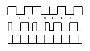
*Bi-phase data stream
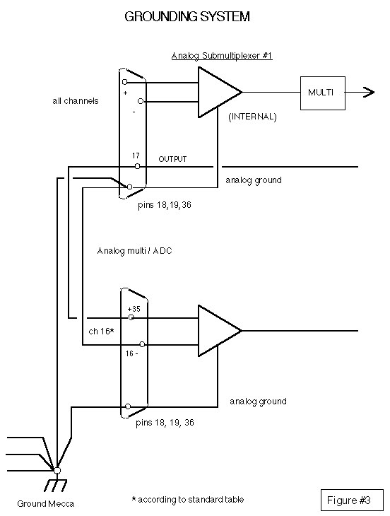
Serial Data Stream (top)
Bi-phased data derived from serial data stream (middle)
Derived from clock transition (bottom)

To get bi-phased data invert value of serial data in the middle of every bit.

      Bi-phase is used because it is easy to derive the clock pulses using phase lock techniques, even when the data is a string of just zeros or ones. i.e. There is a "transition" in the center of every serial bit.

Users Manual


The experimenter has only four controls to adjust:

  1. The ADC full scale trim pot (see figure 1 postscript file) in the Analog Multi/ADC module. This was initially set during check-out. It can be fine adjusted by applying a nearly full scale voltage, about 9V, and adjusting trim pot while watching monitor on ground station.

  2. Choose the Bit rate, usually 32 kHz, sw#7, (see figure 2 postscript file) This switch is in the control module.

  3. Program the Analog Multi/ADC EPROM. See attached sheet for standard program.

  4. Program the Data Frame EPROM in the Control module. It is usual to start with SYNC WORD and end with END OF FRAME (E. of F. word does not appear in serial data stream). Short sample program attached. sample software You might want to consider how the ground station software will decode the data when planning this EPROM.

Notes:

      Each analog submultiplexer's analog output has to be hardwired to one channel of the Analog Multi/ADC module. See attached sheet for one possible system.
      There is an EPROM decoding the multiplexer's address because every analog channel has 17 addresses, its basic address and the 16 addresses of the Analog Sub-Multiplexer wired to it according to the standards system (see attached sheet).
      Each Dual Digital Word Module has to have 2 internal jumpers installed to decide the addresses. If you choose digital word #3 having address (by table) of FD for Word A then the jumper Word A LSB to D and jumper MSB to F. Similar for Word B. Put an adhesive label on each module and note the addresses chosen for each module (Do not have 2 modules with the same address in one system!).
      Each Analog Submultiplexer has one jumper to install. This goes according to the MSB in its address. Note address on adhesive label on exterior of module.
      Do not set Bit Clock slide switch with a pencil tip or graphite will get into the switch's innards and cause you much grief.
      The digital ground has been connected to the digital ground by jumper A (fig. 1). Remove this if you want a fancy ground mecca system.
      Figure 3 or smaller postscript file shows a suitable analog ground arrangement.
See main grounding scheme (postscript file) or see alternate grounding scheme (postscript file)
This documentation written by John Gibson and transcribed by Mike Leung (Oct 1997). Modified and Updated by George Smoot December 1997
This page has been converted from Microsoft Word to HTML byChuck Xiong using vi.
Chuck Xiong can be contacted at: cxiong@uclink4.berkeley.edu